PCB Assembly - OLD

August Electronics > PCB Assembly – OLD

Your manufacturing partner for PCB assembly and beyond.

Our PCB assembly services are the foundation of our business and our experienced team can quickly adapt our SMT lines to assemble simple single layer boards to highly complex multi-layer boards with mixed placement technologies. Whether it’s Through-hole or Surface Mount Technology (SMT) assembly requirements, August has the optimal solution for all your PCB building requirements. We handle designs that are dated as well as those that include the latest lead-free micro BGA technology.

You benefit from our world-class PCB assembly operation in our dedicated 85,000 sq-ft manufacturing facility. We are proudly ISO 9001:2015 certified and committed to continuously improving our processes and operations to consistently provide superior quality products to our clients.

Efficient PCB assembly lines

  • An automatic inline PCB screen printer sits at the front of each SMT line, equipped with an optical system for fiducial alignment and paste inspection.
  • We have both 2D and 3D solder paste inspection (SPI) equipment to ensure reliable SMT placements. In our experience, this critical inspection step plays an important role in minimizing SMT board failures due to poor solder paste release.
  • We run four fully conveyorized SMT machines, consisting of either single or dual head in-line placement machines. These machines are widely used in our industry as they have fast changeover times, vision-guided placement accuracy and intelligent feeder systems.
  • Our automatic in-line pre-reflow inspection machines verify all components have been placed accurately prior to entering the reflow ovens.
  • Each SMT machine is anchored by a 10-zone reflow oven, for maximum control over the reflow profile. Our experienced insertion operators expertly manage your leaded or lead-free assembly needs.
  • Our wave soldering machine utilizes three pre-heating zones to facilitate programmable flux application for soldering. Our experienced technologists can handle your leaded or lead-free assembly requirements.
  • Our selective soldering machine (SSM) utilizes three independent operating zones for maximum throughput, and an electromagnetically operated solder delivery system for near zero-defect solder joints. We also incorporate dual solder pot / alloy configuration to effortlessly switch between leaded and lead-free soldering with minimal setup required.
  • Our 3D automated optical inspection (AOI) verifies solder joint quality and identified defects such as opens, shorts and misaligned or missing components.
  • After completing PCB assembly, the boards are cleaned using our Trident III aqueous wash center. This system generates deionized water in a closed loop system to minimize our environmental impact.
  • We have a rework station is used when intricate board repairs are required. We have lead free capabilities for reworking in-circuit Ball Grid Arrays (BGA), Land Grid Arrays (LGA) or Quad-flat no-leads (QFN).
PCB Assembly Graphic
Inspection stage of manufacturing process
Testing stage of manufacturing process occurring in PCB assembly and box build assemblies

Quality assurance

We maintain the highest standards of quality throughout the assembly process. All circuit board assemblies are barcoded and tracked through the various manufacturing steps. Our team analyzes the data collected at each stage during production to continually enhance and improve the process.

PCB inspection
PCB inspection

A rigorous first article inspection process is performed on each build, complemented by a robust NPI procedure for new products. We produce build documents and machine programs from your information, as well as make recommendations for your designs to streamline your products’ manufacturing process.

Our series of inspections during the PCB assembly process are designed to ensure product quality, reliability and functionality, and to reduce field failures.

Every PCB assembly undergoes:

  • 2D or 3D Solder paste inspection (SPI)
  • Pre-reflow in-line automated optical inspection (AOI)
  • High-resolution 3D AOI inspection
  • Visual inspections
  • X-ray inspection

We invest in the ongoing training and professional development of our production team to keep their knowledge on the cutting edge.

Click the link to learn more about our inspection and testing capabilities.

PCB testing

In addition to our quality assurance inspection steps during the assembly process, all boards have their own individual bar code for full traceability. Our detailed inspection and testing strategies are designed to predict defects in the manufacturing process. This offers you cost efficiencies and confidence in your product’s reliability.

Some of our testing capabilities for PCB assemblies include:

  • In-circuit tests
  • Functional tests
  • Dielectric tests

Click the link to learn more about our inspection and testing capabilities or contact us to discuss your specific inspection and testing requirements.

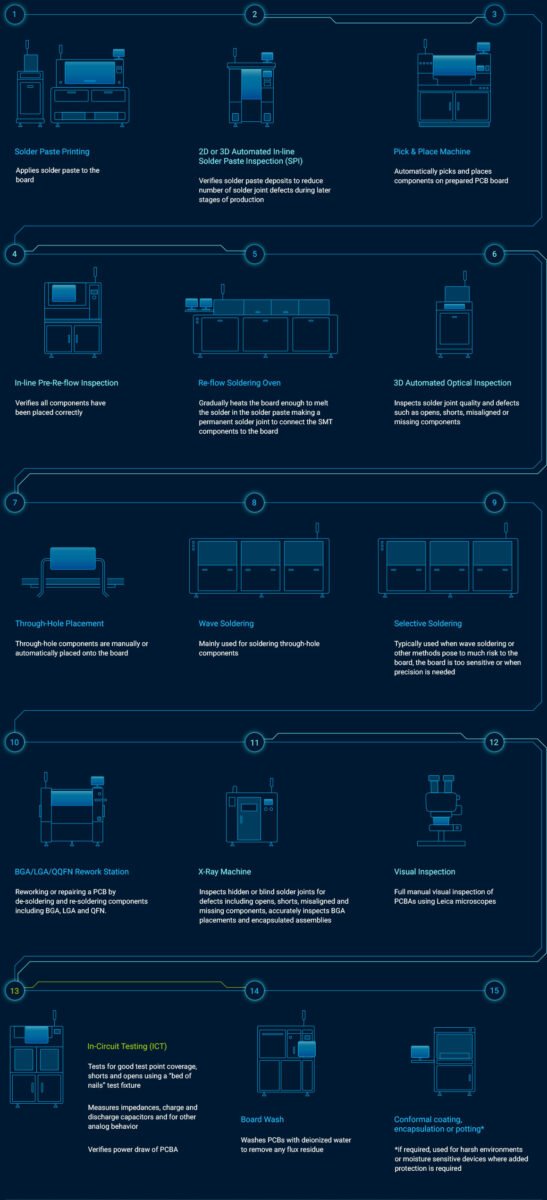
Conformal coating & encapsulation / potting

Conformal coating and encapsulation / potting provides protection to your printed circuit boards (PCB) and box build assemblies against moisture, chemicals, dust and harsh environments with extreme temperature fluctuations.

Our experienced team knows that our clients and their end-users depend on their electronic products and assemblies performing, no matter what kind of rugged environment they are in. As your strategic electronic manufacturing services provider, we recommend the best type of coating material, thickness and coverage that would be required to protect your investment.

We have our standard conformal coat process that utilizes a tri-mode dispensing head with computer controlled selectable dispensing system complete with a conveyorized UV curing oven. The conformal coating process protects your PCBs from moisture and corrosive environments by applying a clear hard coating of acrylated urethane.

Encapsulation / potting is a better option for products or assemblies requiring a more robust form of protection from moisture, corrosion and chemicals. Our standard spray and manual mask application process enables us to apply a wide variety of encapsulation materials such as epoxies and elastomers. Or alternatively, we can work with your engineering team to design and construct jigging or molds during the development of a customized encapsulation process specific to your product or assembly requirements.

To enable future serviceability, our Accuflow micro blasting station utilizes awe can selectively a mild abrasive blasting media such as ground walnut shells to remove the coating to test, repair or upgrade your PCBs and assemblies.

Is your PBC assembly fully optimized?

Whether you are working with another contract electronics manufacturer or building in-house, its worth a second opinion.